Times, Counters and Temperature Controller
Timer, Counter, and Temperature Controller
Jump To Counters Jump To Temperature Contorller
In Future Hi - Tech we sell and Install Timers, Counters and Temperature Controller, Many Type and Many Brands are Available, Please contact us to recommend you with exact type for your application and Offer you best prices
Understanding Time Delay Relay Functions


Issue:
What is the difference between On Delay, Off Delay, Single Shot, Interval On and all these other time delay functions?
Solution/Resolution:
Understanding the differences between all the functions available in time delay relays can sometimes be a daunting task. When designing circuits using time delay relays, questions such as what initiates a time delay relay, does the timing start with the application or release of voltage, when is the output relay energized, etc., must be asked.
Time delay relays are simply control relays with a time delay built in. Their purpose is to control an event based on time. The difference between relays and time delay relays is when the output contacts open & close: on a control relay, it happens when voltage is applied and removed from the coil; on time delay relays, the contacts can open or close before or after some time delay.
Typically, time delay relays are initiated or triggered by one of two methods:
- application of input voltage
- opening or closing of a trigger signal
These trigger signals can be one of two designs:
- a control switch (dry contact), i.e., limit switch, push button, float switch, etc.
- voltage (commonly known as a power trigger)
CAUTION: any time delay relay that is designed to be initiated with a dry contact control switch trigger could be damaged if voltage is applied to the trigger switch terminals. Only products that have a "power trigger" should be used with voltage as the trigger.
To help understand, some definitions are important:
- Input Voltage-control voltage applied to the input terminals. Depending on the function, input voltage will either initiate the unit or make it ready to initiate when a trigger is applied.
- Trigger Signal-on certain timing functions, a trigger is used to initiate the unit after input voltage has been applied. As noted above, this trigger can either be a control switch (dry contact switch) or a power trigger (voltage).
- Output (Load)-every time delay relay has an output (either mechanical relay or solid state) that will open & close to control the load. Note that the user must provide the voltage to power the load being switched by the output contacts of the time delay relay.
Below are both written and visual descriptions on how the common timing functions operate. A Timing Chart shows the relationship between Input Voltage, Trigger (if present) and Output. If you cannot find a product to fit your requirements or have any questions, Future Hi - Tech, Application Engineers offer technical information along with product selection and application assistance. Either This email address is being protected from spambots. You need JavaScript enabled to view it. or call us for help.
| Function | Operation | |
| ON DELAY Delay on Make Delay on Operate |
Upon application of input voltage, the time delay (t) begins. At the end of the time delay (t), the output is energized. Input voltage must be removed to reset the time delay relay & de-energize the output. | |
| INTERVAL ON Interval |
Upon application of input voltage, the output is energized and the time delay (t) begins. At the end of the time delay (t), the output is de-energized. Input voltage must be removed to reset the time delay relay. | |
| OFF DELAY Delay on Release Delay on Break Delay on De-Energization |
Upon application of input voltage, the time delay relay is ready to accept a trigger. When the trigger is applied, the output is energized. Upon removal of the trigger, the time delay (t) begins. At the end of the time delay (t), the output is de-energized. Any application of the trigger during the time delay will reset the time delay (t) and the output remains energized. | |
| SINGLE SHOT One Shot Momentary Interval |
Upon application of input voltage, the time delay relay is ready to accept a trigger. When the trigger is applied, the output is energized and the time delay (t) begins. During the time delay (t), the trigger is ignored. At the end of the time delay (t), the output is de-energized and the time delay relay is ready to accept another trigger. | |
| FLASHER (Off First) |
Upon application of input voltage, the time delay (t) begins. At the end of the time delay (t), the output is energized and remains in that condition for the time delay (t). At the end of the time delay (t), the output is de-energized and the sequence repeats until input voltage is removed. | |
| FLASHER (On First) |
Upon application of input voltage, the output is energized and the time delay (t) begins. At the end of the time delay (t), the output is de-energized and remains in that condition for the time delay (t). At the end of the time delay (t), the output is energized and the sequence repeats until input voltage is removed. | |
| ON/OFF DELAY | Upon application of input voltage, the time delay relay is ready to accept a trigger. When the trigger is applied, the time delay (t1) begins. At the end of the time delay (t1), the output is energized. When the trigger is removed, the output contacts remain energized for the time delay (t2). At the end of the time delay (t2), the output is de-energized & the time delay relay is ready to accept another trigger. If the trigger is removed during time delay period (t1), the output will remain de-energized and time delay (t1) will reset. If the trigger is re-applied during time delay period (t2), the output will remain energized and the time delay (t2) will reset. | |
| SINGLE SHOT FALLING EDGE | Upon application of input voltage, the time delay relay is ready to accept a trigger. When the trigger is applied, the output remains de-energized. Upon removal of the trigger, the output is energized and the time delay (t) begins. At the end of the time delay (t), the output is de-energized unless the trigger is removed and re-applied prior to time out (before time delay (t) elapses). Continuous cycling of the trigger at a rate faster than the time delay (t) will cause the output to remain energized indefinitely. | |
| WATCHDOG Retriggerable Single Shot |
Upon application of input voltage, the time delay relay is ready to accept a trigger. When the trigger is applied, the output is energized and the time delay (t) begins. At the end of the time delay (t), the output is de-energized unless the trigger is removed and re-applied prior to time out (before time delay (t) elapses). Continuous cycling of the trigger at a rate faster than the time delay (t) will cause the output to remain energized indefinitely. | |
| TRIGGERED ON DELAY | Upon application of input voltage, the time delay relay is ready to accept a trigger. When the trigger is applied, the time delay (t) begins. At the end of the time delay (t), the output is energized and remains in that condition as long as either the trigger is applied or the input voltage remains. If the trigger is removed during the time delay (t), the output remains de-energized & the time delay (t) is reset. | |
| REPEAT CYCLE (OFF 1st) |
Upon application of input voltage, the time delay (t1) begins. At the end of the time delay (t1), the output is energized and remains in that condition for the time delay (t2). At the end of this time delay, the output is de-energized and the sequence repeats until input voltage is removed. | |
| REPEAT CYCLE (ON 1st) |
Upon application of input voltage, the output is energized and the time delay (t1) begins. At the end of the time delay (t1), the output is de-energized and remains in that condition for the time delay (t2). At the end of this time delay, the output is energized and the sequence repeats until input voltage is removed. | |
| DELAYED INTERVAL Single Cycle |
Upon application of input voltage, the time delay (t1) begins. At the end of the time delay (t1), the output is energized and remains in that condition for the time delay (t2). At the end of this time delay (t2), the output is de-energized. Input voltage must be removed to reset the time delay relay. | |
| TRIGGERED DELAYED INTERVAL Single Cycle |
Upon application of input voltage, the time delay relay is ready to accept a trigger. When the trigger is applied, the time delay (t1) begins. At the end of the time delay (t1), the output is energized and remains in that condition for the time delay (t2). At the end of the time delay (t2), the output is de-energized & the relay is ready to accept another trigger. During both time delay (t1) & time delay (t2), the trigger is ignored. | |
| TRUE OFF DELAY | Upon application of input voltage, the output is energized. When the input voltage is removed, the time delay (t) begins. At the end of the time delay (t), the output is de-energized. Input voltage must be applied for a minimum of 0.5 seconds to assure proper operation. Any application of the input voltage during the time delay (t) will reset the time delay. No external trigger is required. | |
| ON DELAY/ TRUE OFF DELAY | Upon application of input voltage, the time delay (t1) begins. At the end of the time delay (t1), the output is energized. When the input voltage is removed, the output remains energized for the time delay (t2). At the end of the time delay (t2), the output is de-energized. Input voltage must be applied for a minimum of 0.5 seconds to assure proper operation. Any application of the input voltage during the time delay (t2) will keep the output energized & reset the time delay (t2). No external trigger is required. | |
| SINGLE SHOT-FLASHER | Upon application of input voltage, the time delay relay is ready to accept a trigger. When the trigger is applied, the time delay (t1) begins and the output is energized for the time delay (t2). At the end of this time delay (t2), the output is de-energized and remains in that condition for the time delay (t2). At the end of the time delay (t2), the output is energized and the sequence repeats until time delay (t1) is completed. During the time delay (t1), the trigger is ignored. | |
| ON DELAY-FLASHER | Upon application of input voltage, the time delay begins (t1). At the end of the time delay (t1), the output is energized and remains in that condition for the time delay (t2). At the end of this time delay (t2), the output is de-energized and remains in that condition for the time delay (t2). At the end of the time delay (t2), the output is energized and the sequence repeats until input voltage is removed. | |
| PERCENTAGE | Upon initial application of input voltage, the output is energized and time delay (t1) begins. Time Delay (t1) is adjustable as a percentage of the overall cycle time (t2). At the end of time delay (t1), the output is de-energized for the remainder of overall cycle (t2-t1). The sequence then repeats until input voltage is removed. If input voltage is removed and reapplied, the timing cycle will continue from where it left off when the input voltage was removed. A setting of 100% energizes the output continuously while a setting of 0% de-energizes the output continuously. | |
| PERCENTAGE (NO MEMORY) | Upon initial application of input voltage, the output is energized and time delay (t1) begins. Time Delay (t1) is adjustable as a percentage if the overall cycle time (t2). At the end of time delay (t1), the output is de-energized for the remainder of overall cycle (t2-t1). The sequence then repeats until input voltage is removed. If input voltage is removed and reapplied, the timing cycle will be reset. A setting of 100% energizes the output continuously while a setting of 0% de-energizes the output continuously. |

Understanding Counters Functions
Introduction to Counters – Types of Counters
Counter is a digital device and the output of the counter includes a predefined state based on the clock pulse applications. The output of the counter can be used to count the number of pulses. Generally, counters consist of a flip-flop arrangement which can be synchronous counter or asynchronous counter. In synchronous counter, only one clock i/p is given to all flip-flops, whereas in asynchronous counter, the o/p of the flip flop is the clock signal from the nearby one. The applications of the microcontroller need counting of exterior events such as exact internal time delay generation and the frequency of the pulse trains. These events are frequently used in digital systems & computers. Both these events can be executed by software techniques, but software loops for counting will not give the exact result slightly more important functions are not done. These problems can be rectified by timers and counters in the microcontrollers which are used as interrupts.
Types of Counters
Counters can be categorized into different types according to the way they are clocked. They are
- Asynchronous Counters
- Synchronous Counters
- Asynchronous Decade Counters
- Synchronous Decade Counters
- Asynchronous Up-Down Counters
- Synchronous Up-Down Counters
For better understanding of this type of counters, here we are discussing some of the counters.
Asynchronous Counters
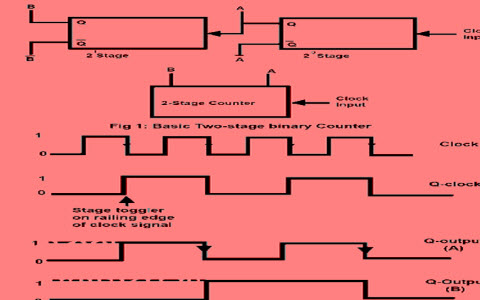
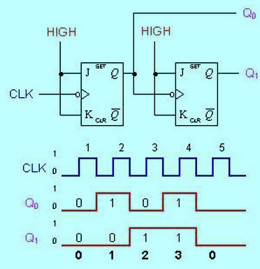
The diagram of a 2-bit asynchronous counter is shown below. The exterior clock is connected to the clock i/p of the FF0 (first flip-flop) only. So, this FF changes the state at the decreasing edge of every clock pulse, but FF1 changes only when activated by the decreasing edge of the Q o/p of FF0. Because of the integral propagation delay through a FF, the change of the i/p clock pulse and a change of the Q o/p of FF0 can never occur at precisely the same time. So, the FF’s cannot be activated concurrently, generating an asynchronous operation.
Note that for ease, the changes of Q0,Q1 & CLK in the above diagram are shown as concurrent, even though this is an asynchronous counter. Actually, there is a small delay b/n the Q0, Q1 and CLK changes.
Generally, all the CLEAR i/ps are connected together, so before counting starts then that a single pulse can clear all the FFs. The clock pulse fed into FF0 is rippled through the new counters after propagation delays, such as a ripple on the water, hence the term Ripple Counter.
The circuit diagram of the two bit ripple counter includes four different states ,each one consisting with a count value. Likewise, a counter with n FFs can have 2N states. The number of states in a counter is called as its mod number. Therefore a two-bit counter is a mod-4 counter.
Asynchronous Decade Counters
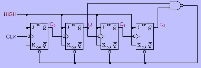
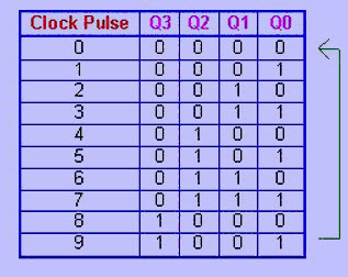
In the previous counter have 2n states. But, counters with states less than 2n is also possible. These are designed to have the no. of states in their series.These are called shortened sequences which are accomplished by driving the counter to recycle before going through all of its states. A common modulus for counters with shortened sequence is 10. A counter with 10-states in its series is called a decade counter.The implemented decade counter circuit is given below.
When the counter counts to ten, then all the FFs will be cleared. Notice that only Q1&Q3 both are used to decode the count of 10, that is called partial decoding. At the same time one of the other states from 0-9 have both Q1&Q3 will be high. The series of the decade counter table is given below.
Asynchronous Up-Down Counters
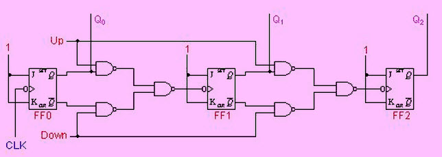
In particular applications, a counter must be capable to count both up & down. The below circuit is a three bit up & down counter, that counts UP or DOWN based on the control signal status. When the UP i/p is at 1 & the DOWN i/p is at 0, the NAND gate between FF0 & FF1 will gate the non-inverted o/p (Q) of flip flop (FF0) into the clock i/p of flip flop (FF1). Likewise, the non-inverted o/p of Flip Flop1 will be gated through the other NAND gate into the clock i/p of flip-flop2. Therefore the counter will count up.
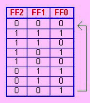
Once the control i/p (UP) is at 0 & DOWN is at 1, the inverted o/ps of flip-flop0 (FF0) and flip-flop1 (FF) are gated into the clock i/ps of FF1 & FF2 separately. If the FFs are initially changed to 0’s, then the counter will go through the below series as i/p pulses are applied. Notice that an asynchronous up-down counter is slower than an UP counter/down counter because of an extra propagation delay introduced by the NAND gates.
Synchronous Counters
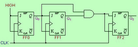
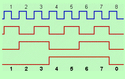
In this type of counters, the CLK i/ps of all the FFs are connected together and are activated by the i/p pulses. So, all the FFs change states instantaneously. The circuit diagram below is a three bit synchronous counter. The inputs J and K of flip-flop0 are connected to HIGH. Flip-flop 1 has its J &K i/ps connected to the o/p of flip-flop0 (FF0), and the inputs J & K of flip-flop2 (FF2) are connected to the o/p of an AND gate that is fed by the o/ps of flip-flop0 and flip-flop1. When the both the outputs of FF0 & FF1 are HIGH. The positive edge of the fourth CLK pulse will cause FF2 to alter its state because of the AND gate.
The series of the three bit counter table is given below.The major advantage of these counters is that there is no increasing time delay due to all FFs are activated in parallel. Thus, the max operating frequency of this synchronous counter will be considerably higher than for the equivalent ripple counter.
Synchronous Decade Counters
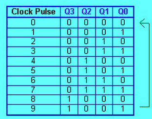
Synchronous counter counts from 0-9 similar to asynchronous counter and then again recycles zero. This process is done by driving the 1010 states back to the 0000 state. This is termed as truncated sequence, that can be designed by the below circuit.
From the series on the left table, we can observe that
- Q0 ties on each and every CLK pulse
- Q1 alters on the next clock pulse every time when Q0=1 & Q3=0.
- Q2 alters on the next clock pulse every time when Q0=Q1=1.
- Q3 alters on the next CLK pulse each and every time when Q0=1, Q1=1 & Q2=1 (count 7), or when Q0=1 & Q3=1 (count 9).
The above characteristics are employed with the AND gate or OR gate. The logic diagram of this is shown in the above diagram.
Synchronous Up-Down Counters
A three bit synchronous Up-Down counter, tabular form and series are given below. This type of counter has an up-down control i/p similar to asynchronous up-down counter, that is used to control the counter’s direction through a certain series.
The series of the table shows
- Q0 ties on each CLK pulse for both up & down series
- When Q0=1 for the up series, then the state of the Q1 changes on the next CLK pulse.
- When Q0=0 for the down series, then the state of the Q1 changes on the next CLK pulse.
- When Q0=Q1=1 for the up series, then the state of the Q2 changes on the next CLK pulse.
- When Q0=Q1=0 for the down series, then the state of the Q2 changes on the next CLK pulse.
The above characteristics are employed with the AND gate, OR gate and NOT gate. The logic diagram of this is shown in the above diagram.
Applications of Counters
The applications of the counters mainly involve in digital clocks and in multiplexing. The best example of the counter is parallel to serial data conversion logic discussed below.
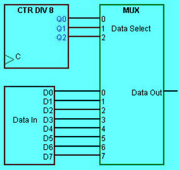
A set of bits, performing concurrently on parallel lines is called parallel data. A set of bits, performing on a single line in a time series is called serial data. The Parallel-to-serial data conversion is normally is done by using a counter to afford a binary series of the data, select i/ps of a MUX, as explained in the circuit below.
In the above circuit, modulo-8 counter consist of Q o/ps, that are connected to the data, select i/ps of an 8-bit MUX. The first 8-bit group of parallel data is applied to the inputs of the MUX. As the counter goes through a binary series from 0-7, each bit starts with D0, is serially selected & passed through the MUX to the o/p line. After 8-CLK pulses, the data byte has been changed to a serial format & sent out through the transmission line. Then, the counter reprocesses back to 0 and changes another parallel byte serially again in the similar process.
Thus, this is all about the counters and types of counter, which includes Asynchronous Counters, Synchronous Counters, Asynchronous Decade Counters, Synchronous Decade Counters, Asynchronous Up-Down Counters and Synchronous Up-Down Counters.

